Commodity Hardware today
Over the years personal computers and smaller servers standardized on a chipset with two parts: the Northbridge and Southbridge.
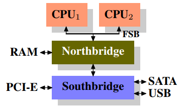
A couple of bottlenecks are immediately apparent in this design
RAM bandwidth 争抢 (DMA 允许 device 直接从 RAM 里读写数据,但是都要通过 Northbridge,这样就 CPU 通过 Northbridge 访问 RAM 的 bandwidth冲突)
In the earliest days of the PC, all communication with devices on either bridge had to pass through the CPU, negatively impacting overall system performance. To work around this problem some devices became capable of direct memory access (DMA). DMA allows devices, with the help of the Northbridge, to store and receive data in RAM directly without the intervention of the CPU (and its inherent performance cost). Today all high-performance devices attached to any of the buses can utilize DMA. While this greatly reduces the workload on the CPU, it also creates contention for the bandwidth of the Northbridge as DMA requests compete with RAM access from the CPUs.
因为有限的 Northbandwidth,所以需要 schedule memory access in ways that minimize delays.
On some more expensive systems, the Northbridge does not actually contain the memory controller. Instead the Northbridge can be connected to a number of external memory controllers (外接 memory controller)
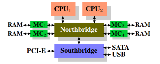
Pros:
- more than one memory bus, so the bandwitdth increases
- support memory
Concurrent memory access patterns reduce delays by simultaneously accessing different memory banks. This is especially true when multiple processors are directly connected to the Northbridge. For such a design, the primary limitation is the internal bandwidth of the Northbridge.
除了上述提升 memory bandwidth 的办法,还有一种,就是将 memory controller 嵌入到 CPU,并将 memory attached 到 CPU 上
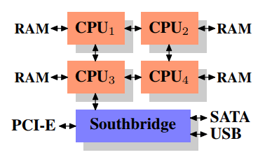
AMD的 Opteron processor 就是这样,另外 Intel 支持的 Common System Interface (CSI) Nehalem processor 也是差不多的原理。(NUMA - Non-Uniform Memory Architecture)
Cons:
- RAM 不再 uniform, 从 CPU1访问 CPU2 的RAM,会要求一次 CPU 的 interconnect,如果是 CPU1 访问 CPU4,则会要求 2次 interconnects
RAM Type
Static RAM
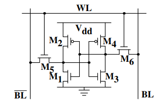
The core of this cell is formed by the four transistors $M1$ to $M4$ which form two cross-coupled inverters. They have two stable states, representing 0 and 1 respectively. The state is stable as long as power on $Vdd$ is available.
the cell state is stable, no refresh cycles are needed
Dynamic RAM
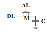
To read the state of the cell the access line $AL$ is raised; this either causes a current to flow on the data line $DL$ or not, depending on the charge in the capacitor.
To write to the cell the data line$DL$ is appropriately set and then $AL$ is raised for a time long enough to charge or drain the capacitor.
Cons:
Leakage problem
The use of a capacitor means that reading the cell discharges the capacitor. The procedure cannot be repeated indefinitely,the capacitor must be recharged at some point. Capacity of the capacitor is low, it only takes a short time for the capacity to dissipate.
This leakage is why a DRAM cell must be constantly refreshed. For most DRAM chips these days this refresh must happen every 64ms. During the refresh cycle no access to the memory is possible since a refresh is simply a memory read operation where the result is discarded. For some workloads this overhead might stall up to 50% of the memory accesses- information read is not directly usable. A sense amplifier is used to distinguish between 0 and 1
- A third problem is that reading a cell causes the charge of the capacitor to be depleted. This means every read operation must be followed by an operation to recharge the capacitor. It does mean, though, the reading memory content
requiresadditional energy and,more importantly, time. - A fourth problem is that charging and draining a capacitor is not instantaneous.
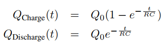
Unlike the static RAM case where the output is immediately available when the word access line is raised, it will always take a bit of time until the capacitor discharges sufficiently. This delay severely limits how fast DRAM can be.
The speed can vary from only slightly slower than the CPU core to one or two orders of magnitude slower. SRAM 的性能差异很大,可能只比 CPU core 慢一点,或者慢 1-2 个数量级
DRAM Access Technical Details
Synchronous DRAM (SDRAM) and its successors Double Data Rate DRAM (DDR)
Synchronous DRAM, as the name suggests, works relative to a time source. The memory controller provides a clock, the frequency of which determines the speed of the Front Side Bus (FSB) – the memory controller interface used by the DRAM chips. As of this writing, frequencies of 800MHz, 1,066MHz, or even 1,333MHz are available with higher frequencies (1,600MHz) being announced for the next generation. This does not mean the frequency used on the bus is actually this high. Instead, today’s buses are double- or quad-pumped, meaning that data is transported two or four times per cycle. Higher numbers sell so the manufacturers like to advertise a quad-pumped 200MHz bus as an “effective” 800MHz bus
For SDRAM today each data transfer consists of 64 bits – 8 bytes. The transfer rate of the FSB is therefore 8 bytes multiplied by the effective bus frequency (6.4GB/s for the quad-pumped 200MHz bus).
Read Access Protocol
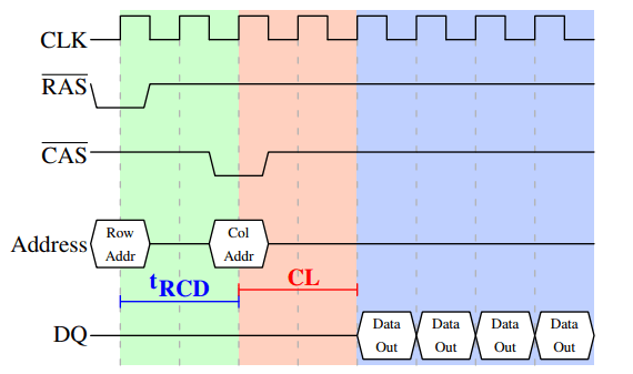
bus clock, RAS and CAS signals, and the address and data buses.
A read cycle begins with the memory controller making the row address available on the address bus and lowering the RAS signal. All signals are read on the rising edge of the clock (CLK) so it does not matter if the signal is not completely square as long as it is stable at the time it is read. Setting the row address causes the RAM chip to start latching the addressed row.
The CAS signal can be sent after tRCD (RAS-to-CAS Delay) clock cycles. The column address is then transmitted by making it available on the address bus and lowering the CAS line.
With all this preparation to get to the data it would be wasteful to only transfer one data word. This is why DRAM modules allow the memory controller to specify how much data is to be transmitted. Often the choice is between 2, 4, or 8 words. This allows filling entire lines in the caches(cache line) without a new RAS/CAS sequence